
3D Imaging of Interconnects
Three-dimensional imaging of nanovoids, roughness and critical dimensions in electrical interconnects using electron tomography.
A more detailed technical description of this work can be found here and here.
These projects are performed in collaboration with our partners at AMD, Applied Materials, IBM, Intel and Novellus. The work is funded by the Semiconductor Research Corporation and its member companies and NYSTAR, with facilities support from the National Science Foundation.
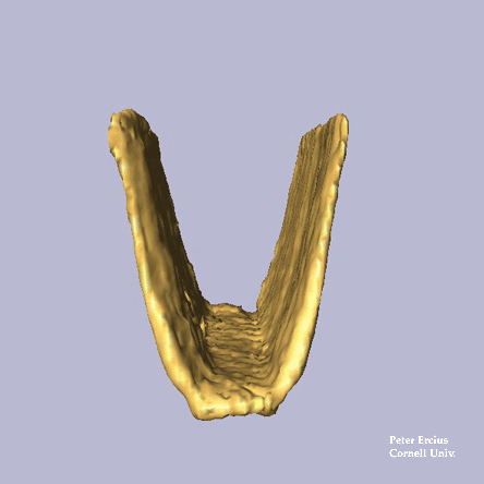
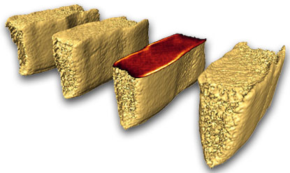
Three-dimensional reconstruction of a tantalum liner around a copper wire used to connect transistors together in a computer chip.
Note the sidewall roughness, which is probably a residual of the roughness from the lithographic mask used to define the interconnect itself.